Equipment
Equipment
Superconductor Wire Manufacturing
-
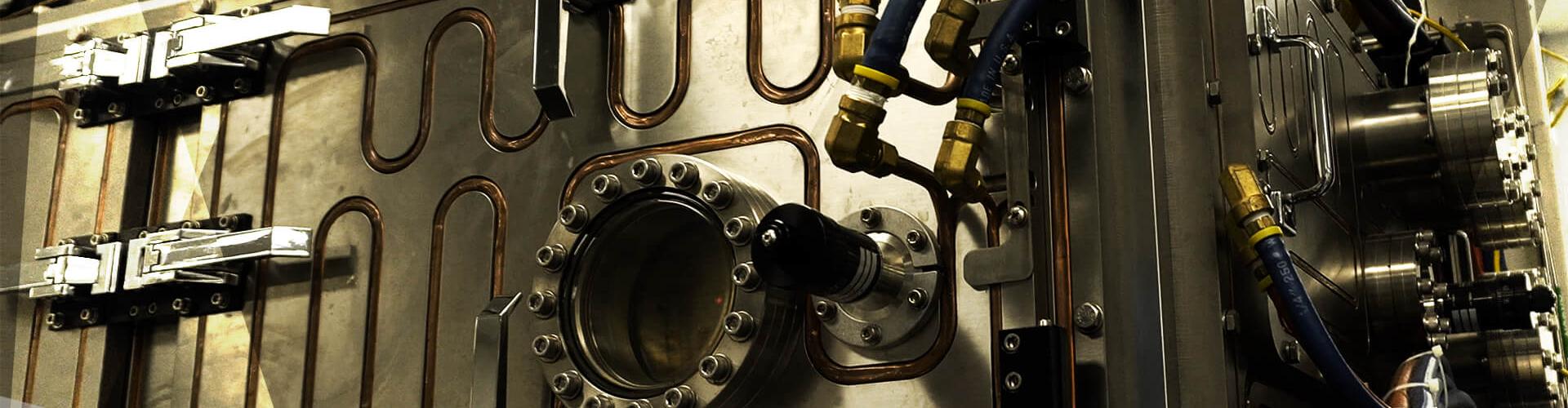
Pilot-scale superconductor metal organic chemical vapor deposition tool (MOCVD)
-
Used to conduct manufacturing research, the pilot-scale superconductor metal organic chemical vapor deposition tool (MOCVD) features:
- Meter-long deposition zone
- Nine-track helix tape winding for simultaneous deposition over nine tape tracks
- Dual high capacity evaporators
- Dual high capacity pumping system
- In-line X-ray Diffraction for real time information on crystallographic orientation of superconductor film growth
- In-line vision system for real-time detection and tagging of defects in the film
-
-
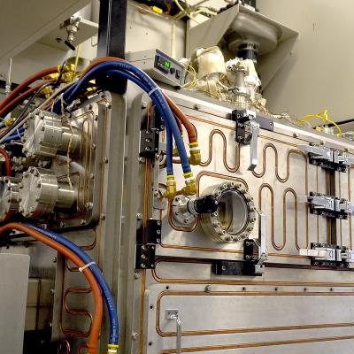
Advanced MOCVD tool
-
Provides excellent stability of film growth temperature, precursor composition and high precursor-to-film conversion efficiency. The advanced MOCVD tool features a novel reactor design that includes:
-
Direct tape heating
-
Direct temperature monitoring
-
Laminar flow channel
-
Plasma activation
-
-
-
Reel-to-reel system electropolishing and electroplating system
-
Used for electro polishing of substrates and electroplating system of copper stabilization on long superconductor tapes and magnetron sputtering of silver over layer on superconductor wires.
-
-
Reel-to-reel scanning hall probe microscope (SHPM)
-
This tool is used for high-resolution critical current mapping of long tapes produced in our manufacturing research as well as those manufactured by industry. The reel-to-reel SHPM features:
-
High speed, high resolution driver for a hall probe that maps the magnetic field and in turn the critical current of the tape.
-
A spatial resolution of 100 µm is achievable even at a linear tape speed of 30 m/h. "
-
-
-
Reel-to-reel system for magnetron sputtering of silver
-
This system was designed and built in house. It can be used for magnetron sputtering of silver and other materials as well, on a manufacturing scale.
-
-
Reel-to-reel wire winding equipment
-
UH and its industrial partner AMPeers designed, constructed and commissioned a reel-to-reel wire winding system in our facility for spiral winding of superconductor tapes to fabricate round, ultra-small diameter wires.
-
-
Reel-to-reel in-field critical current measurement system for long superconductor tapes
-
The critical current of long superconductor tapes is measured in a magnetic field of 5 Tesla. This equipment provides unique performance data that is important for verification of uniformity of quality of superconductor tapes in many applications but has not been available even in industry. Using know-how that was developed in our research laboratories, we established this innovative tool to qualify long tapes that are produced in our manufacturing research as well as those made in industry.
-
Roll-to-roll Semiconductor Manufacturing
-
Roll-to-roll thin film deposition system
- Used to conduct manufacturing research, the roll-to-roll thin film deposition system features:
- Two ion beam assisted deposition (IBAD)
- Three magnetron sputtering
- One e-beam evaporation systems.
- Used to conduct manufacturing research, the roll-to-roll thin film deposition system features:
-
Roll-to-roll MOCVD of III-V thin films
-
This tool is very likely the first roll-to-roll compound semiconductor MOCVD system ever to be built in the world. The roll-to-roll MOCVD of III-V thin films features dual reactors:
-
Dual reactors: one for roll-to-roll processing of 100m long, 50 mm wide flexible substrates and another for 50 mm diameter wafers
-
Delivery of six metal organic and six hydrides precursors, deposition temperature capability up to 1300 C and 600 W plasma sources.
-
All necessary features for safe operation.
-
-
-
Plasma enhanced chemical vapor deposition (PECVD) tools
-
The plasma enhanced chemical vapor deposition (PECVD) tools features dual reactors:
-
One for epitaxial germanium and silicon deposition
-
One for dielectric deposition.
-
-
-
Other Tools
-
Complete semiconductor device fabrication equipment including sputter, e-beam and thermal evaporation systems and lithography tools are available in the device fabrication area. Photolithographic tools for semiconductor device fabrication is present in a separate device fabrication area .
-
Metrology Tools
-
Other tools
-
Several advanced metrology tools are available in our Semiconductor Device Fabrication laboratory. These include:
-
Bruker X-ray Diffractometer (XRD) with area detector
-
Bruker High Resolution XRD system
-
Agilent Inductively Coupled Plasma Spectroscopy (ICP-MS)
-
Stylus and Optical profilometers.
-
Solar cell conversion efficiency measurements system including a AAA Solar simulator with concentrated light
-
internal and external quantum efficiency measurement system
-
Hall mobility, time-resolved photoluminescence measurement systems
-
Electromagnetic testing apparatus (Capability for various measurements –1T, 9T/Capability for various temperatures – 4.2K to 77K) 170 angular orientation between the magnetic field and superconductor tape is also available.
-
Physical property measurement system (PPMS) – Capable of magnetization and susceptibility measurements from 4.2K to 77K in magnetic fields up to 14 T.
-
-
CONTACT US
UH Technology Bridge
Building 15
5000 Gulf Freeway
Houston, TX 77023
Phone: 713-743-4044
Email: selva@uh.edu